Close
We enable business and digital transformation decisions through the delivery of cutting-edge ICT solutions and products...
The move to 5nm means 30 billion transistors on a chip the size of a fingernail and all the performance potential that brings with it.
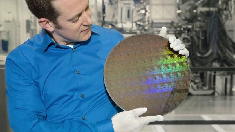
Some of the major performance breakthroughs in chip design have come about by shrinking the die size. It means fitting more in less space, and it’s measured in nanometers. Today’s processors found inside desktop PCs and laptops are typically 14nm chips, with the next jump being 10nm. However, IBM is looking to the future. Two years ago it developed a 7nm process, but today the company announced an industry-first process for building 5nm chips.
The new process will be presented in detail at the 2017 Symposia on VLSI Technology and Circuits conference in Kyoto, Japan this week. IBM worked with partners Samsung and Globalfoundries to achieve the breakthrough, which ditched the commonly used FinFET architecture replacing it instead with stacks of silicon nanosheets. IBM worked to perfect nanosheet semiconductor technology for over a decade.
The 5nm process was demonstrated by producing silicon nanosheet transistors at the SUNY Polytechnic Institute Colleges of Nanoscale Science and Engineering NanoTech Complex in Albany, NY. By doing so, it proves that 5nm is possible and paves the way for its adoption once 10nm and 7nm are exhausted.
That could be years away as 7nm is only set to be commercialized in 2018 at IBM’s Fab 8 manufacturing facility. Based on the 7nm timeline that suggests 5nm will come online around 2020.
As for performance, IBM claims there are significant gains when compared to 10nm chips. Performance enhancement from the jump to 5nm is 40 percent at fixed power. Alternatively, there’s a 75 percent power saving on offer. Whichever way you look at it, 5nm will be highly desirable in devices ranging from smartphones and tablets through to the Internet of Things, rooms full of servers, and AI.
If you’re wondering why IBM moved away from the FinFET transistor architecture, the company readily admits FinFET will scale to 5nm. However, while the size scales the performance does not. Shifting to an Extreme Ultraviolet (EUV) lithography technique as used for its 7nm process allows the nanosheets to be constantly adjusted. By doing that, performance and power fine-tuning can be carried out on a per-circuit basis. Ultimately you end up with higher performance 5nm chips thanks to EUV.
Gideon Ebonde M. is the CEO and Chief Software Architect at Musato Technologies. He is experienced Software developer with a demonstrated history of working in the information technology and services industry. He has a strong engineering professional skilled in Mobile Application Development, Enterprise Software, AI, Robotics, IoT, Servers, Cloud and business application. He is an accomplished DevOps software engineer and a visionary computer scientist and engineer.